Manufacturing Solutions for the Semiconductor Industry
Semiconductor manufacturing produces microchips and integrated circuits through ultra-precise fabrication processes in cleanroom environments with nanometer-scale tolerances.
Required Certifications
Key Industry Challenges
Manufacturing Processes for Semiconductor
CNC Machining
Computer Numerical Control machining uses programmed commands to control cutting tools that shape metal and plastic parts with extreme precision. It is one of the most versatile and widely used manufacturing processes in the world.
5-Axis Machining
5-axis machining moves a cutting tool along five axes simultaneously, enabling the creation of extremely complex parts in a single setup with superior precision and surface quality.
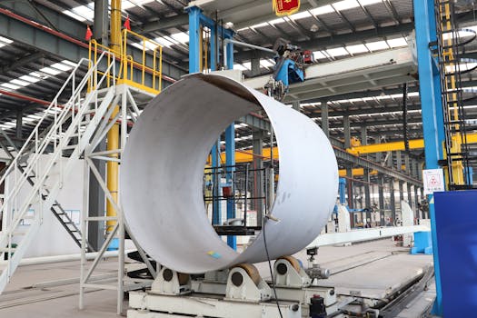
Sheet Metal Fabrication
Sheet metal fabrication combines cutting, bending, and assembly operations to transform flat sheets into enclosures, brackets, panels, and structural components.
Laser Cutting
Laser cutting uses a focused, high-powered laser beam to cut through metals, plastics, and other materials with extreme precision, speed, and minimal material waste.
Surface Finishing
Surface finishing processes improve the appearance, corrosion resistance, wear resistance, and functionality of manufactured parts through coatings, treatments, and polishing.
Anodizing
Anodizing creates a controlled oxide layer on aluminum parts through an electrochemical process, providing excellent corrosion resistance, wear resistance, and color options.
Plating
Plating deposits a thin layer of metal (zinc, nickel, chrome, gold, silver) onto parts for corrosion protection, wear resistance, conductivity, and aesthetics.
Wire EDM
Wire EDM uses a thin electrically charged wire to cut through conductive metals with extreme precision, producing intricate shapes and tight tolerances impossible for conventional machining.
Grinding
Grinding uses abrasive wheels to remove small amounts of material with extreme precision, achieving tight tolerances and superior surface finishes on hardened metals.
Extrusion
Extrusion forces heated metal or plastic through a shaped die to create long parts with consistent cross-sections like profiles, tubes, channels, and structural shapes.
Semiconductor Manufacturing FAQ
What precision is needed for semiconductor manufacturing equipment?
Semiconductor equipment components require tolerances of ±0.0001" (2.5μm) or tighter. Surface finishes must be 4-8 Ra microinches. Materials must be ultra-clean with minimal outgassing. Equipment chambers are often electropolished stainless steel or anodized aluminum.
What materials are used in semiconductor equipment?
Anodized aluminum (6061-T6) is used for vacuum chambers and wafer handling. Stainless steel (316L electropolished) is used for gas delivery. Quartz, silicon carbide, and ceramics are used for high-temperature process components. Teflon and PEEK for chemical-resistant components.
Why are semiconductor fabs so expensive?
A modern semiconductor fab costs $10-20+ billion due to extreme precision lithography equipment (EUV), cleanroom construction and maintenance, ultra-pure chemical and gas delivery systems, and the hundreds of specialized tools required for the fabrication process.
Generate Semiconductor Manufacturing Leads
Tell us about your manufacturing capabilities and we'll show you exactly how to attract qualified buyers. No obligation.
Tell Us About Your Semiconductor Capabilities →